
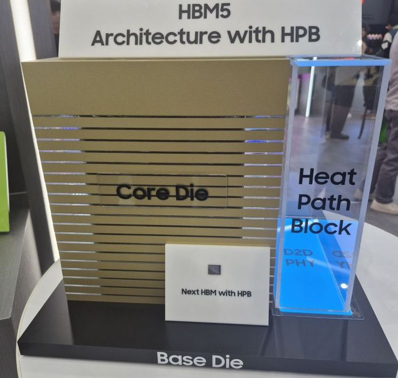
Samsung unveiled an HBM5 stack memory prototype at Computex 2026.
Samsung Electronics – First Steps Toward HBM5
Recently Samsung Electronics announced the start of deliveries of HBM4E memory samples, but at the same time it is already actively developing the next generation – HBM5. At Computex 2025, the company showed only a large-scale mock-up of an HBM5 chip to give a general idea of its structure. Even now it is clear that the technology will be complex and demanding.
Key Development Details
Parameter What Samsung Does Basic Crystal Self‑manufacturing on a 2‑nm process Number of DRAM layers From 12 to 20 (class 1c technology) GAA Transistors Planned for use in 2‑nm chips Process below 1 nm The company is confident it will master it in the future
Technical director of Samsung Electronics’ division, Song Jaehyuk, confirmed the company's participation in developing and implementing these technologies. Having a contract unit allows meeting the requirements of the most demanding clients, including Nvidia.
Comparison with HBM4E
* HBM4E uses a 4‑nm basic crystal and a 1c process to manufacture DRAM chips that form the memory stack.
* HBM5 will offer:
* A thinner crystal (2 nm) and a more flexible number of layers (12–20).
* Heat Path Block (HPB) – a heat‑dissipation channel for efficient cooling.
* Increased data transfer speed thanks to an improved architecture.
The HPB technology is already refined on the HBM4E example, and Samsung plans to use advanced heat‑dissipation methods to improve memory stability. Mass production of HBM5 is planned from 2028, and within HBM5E DRAM crystals will be produced using a more advanced 1d process.
What Competitors Are Doing
* SK hynix uses a similar cooling technology – iHBM. This means Samsung’s solution is not unique in terms of heat dissipation.
* SK hynix also implements 2‑nm chips as part of HBM5 and plans mass production using iHBM.
Conclusion
Samsung Electronics is already developing HBM5 on a 2‑nm process, allowing up to 20 DRAM layers and the innovative HPB heat‑dissipation system. Mass production is scheduled for 2028, and competitors such as SK hynix use similar solutions (iHBM). Overall, Samsung demonstrates confidence in mastering sub‑1 nm technologies and readiness to meet the demands of its largest clients.
 Asted Cloud
Comments (0)
Share your thoughts — please be polite and stay on topic.
Log in to comment